
Understanding the Semiconductor Manufacturing Process: Key Techniques and Innovations in Semiconductor Fabrication and Device Manufacturing
Overview of the Semiconductor Manufacturing Process
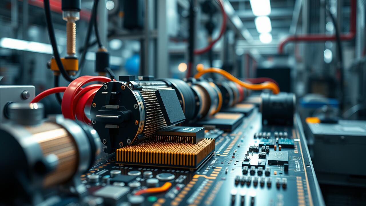
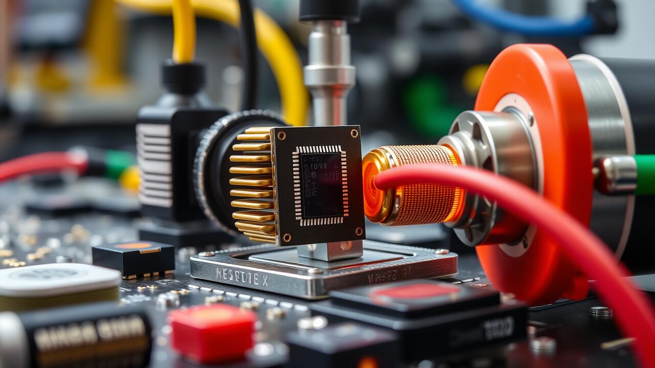
The semiconductor manufacturing process is a complex series of steps that create the intricate circuitry of semiconductor devices. This fabrication process begins with wafer fabrication, where silicon or other materials are shaped and prepared for further processing. Each stage, including doping, ion implantation, and photolithography techniques, is crucial to achieving the desired electrical properties. Advanced semiconductor manufacturing relies on sophisticated semiconductor manufacturing equipment to ensure precision and efficiency. The successful execution of these semiconductor processes leads to the production of high-performance semiconductor chips, essential for various applications in modern technology and electronics. As the demand for innovative solutions grows, the semiconductor manufacturing technology continues to evolve, pushing the boundaries of what’s possible in semiconductor device manufacturing.
Definition and Importance of Semiconductors
Semiconductors are essential components in modern electronics, serving as the building blocks for a vast array of devices. The semiconductor manufacturing process involves intricate steps that transform raw materials into functional devices. These processes enable the production of integrated circuits and microchips, which are integral to everything from computers to smartphones. Semiconductor manufacturers play a crucial role in shaping the semiconductor industry, continually innovating to enhance semiconductor device fabrication.
The significance of semiconductors extends beyond their function in electronics. Semiconductor processing has revolutionized various sectors, including telecommunications, automotive, and healthcare. The fabrication of semiconductor devices takes place in specialized semiconductor fabrication plants that utilize advanced technologies to ensure precision and efficiency. As demand for technology increases, the semiconductor industry’s ability to meet these challenges relies heavily on efficient semiconductor fabrication and robust manufacturing processes.
Key Steps in the Semiconductor Manufacturing Process
The semiconductor manufacturing process involves multiple stages that transform raw semiconductor materials into functional devices. Each step in the semiconductor fabrication plants is crucial to achieving the desired semiconductor properties. These fabrication processes include doping, etching, and deposition, which are essential for creating intricate structures on semiconductor wafers. Understanding these steps helps to appreciate how semiconductor devices are made and the complexities involved in chip manufacturing.
Quality control is vital throughout the semiconductor manufacturing process to ensure the reliability of semiconductor devices. Industry standards set forth by organizations such as the semiconductor industry association play a significant role in maintaining product integrity. Innovations in technologies and materials continue to drive advancements in the semiconductor industry, enabling manufacturers to produce chips with enhanced performance and efficiency. This ongoing evolution is essential for meeting the growing demands of various applications across sectors.
- Doping introduces impurities into semiconductor materials to modify electrical properties.
- Etching creates patterns on the wafer surface by removing specific areas of material.
- Deposition involves adding thin layers of materials onto the wafer for various functions.
- Photolithography is used to transfer patterns from masks to semiconductor wafers.
- Chemical mechanical polishing (CMP) ensures a smooth and even wafer surface.
- Quality control checks include testing for defects and ensuring process consistency.
- Continuous innovation in materials and techniques is crucial for improving chip performance.
Stages of Semiconductor Manufacturing
The semiconductor manufacturing process consists of several critical stages that transform raw materials into sophisticated semiconductor chips. Wafer fabrication serves as the foundation, where the semiconductor material is shaped and prepared for subsequent processing. Doping and ion implantation introduce essential impurities, altering the electrical properties to create p-type or n-type regions. Photolithography techniques then define intricate patterns on the wafer, paving the way for the formation of integrated circuits. Following this, etching and deposition processes help refine these structures, ensuring that the features meet the required specifications for functionality. Each of these stages relies heavily on advanced semiconductor equipment and materials international, underscoring the essential role of semiconductor foundries in the overall manufacturing ecosystem. The culmination of these processes results in the production of semiconductor packages that house the integrated circuits, ready for deployment in various applications.

Wafer Fabrication
The semiconductor manufacturing process begins with the creation of a semiconductor wafer, a thin slice of semiconductor material, often silicon. This wafer serves as the foundational substrate for chip fabrication, which includes all subsequent steps. Fairchild Semiconductor played a pivotal role in advancing the technology for fabricating these wafers, particularly in the development of metal-oxide semiconductors and n-type semiconductors. These innovations laid the groundwork for modern semiconductor memory and other electronic components that form the backbone of contemporary technology.
Fabrication facilities are equipped with sophisticated machinery to ensure precision during wafer processing. The transformation of intrinsic semiconductors into functional devices involves multiple stages, including doping and patterning techniques. The process relies heavily on controlling the properties of semiconductor wafers with high accuracy to achieve desired electrical characteristics. This level of detail is crucial as the demands for performance and miniaturization grow in today’s electronics-driven world.
Doping and Ion Implantation
Doping and ion implantation are critical steps in the semiconductor manufacturing process that enhance the electrical properties of semiconductor materials. By introducing impurities into the silicon wafers, these techniques enable the creation of p-type and n-type semiconductors, essential for developing various semiconductor products. This specific semiconductor process takes place in highly controlled environments within semiconductor fabrication facilities, where precision is paramount. Recent innovations in this area have been discussed extensively at semiconductor manufacturing conferences, showcasing advancements that contribute to more efficient industrial semiconductor fabrication.
The significance of these processes extends beyond traditional methods to include new semiconductor processes aimed at improving performance and yield. Challenges faced by global players, including those in Chinese semiconductor manufacturing, highlight the importance of innovations in doping and ion implantation. Home semiconductor manufacturing enthusiasts also benefit from understanding these concepts as they seek to replicate aspects of the professional semiconductor manufacturing process in smaller-scale settings. As demand for advanced semiconductor products continues to grow, optimizing doping and ion implantation techniques remains a focal point for researchers and manufacturers alike.
Photolithography Techniques
Photolithography serves as a cornerstone in the semiconductor manufacturing process, enabling the precise transfer of intricate patterns onto silicon wafers. This technique evolved from early semiconductor processes and has been crucial in specialized semiconductor fabrication. Many semiconductor manufacturers rely on photolithography to achieve the accuracy required for advanced semiconductor designs. The quality of the photolithography equipment directly impacts the effectiveness of semiconductor device fabrication, making it a vital area of focus for semiconductor engineering.
The advancements in photolithography techniques have significantly influenced the efficiency of the semiconductor industry trade and the overall semiconductor supply chain. High-resolution imaging and improved optical systems allow for the miniaturization of devices, which is essential for meeting the demands of modern technology. As the manufacturing process becomes more complex, continuous innovations in photolithography address challenges and propel advancements within the semiconductor manufacturing process. These developments ensure that the industry remains competitive and responsive to market needs.
Etching and Deposition Processes
Etching and deposition are pivotal steps in the semiconductor manufacturing process, essential for defining intricate patterns on wafers. Through these various fabrication processes, many semiconductor companies utilize advanced semiconductor solutions to manipulate the underlying semiconductor material. This precision impacts semiconductor device performance, making it crucial for the evolving global semiconductor industry. By employing cutting-edge semiconductor capital equipment, the etching and deposition stages enable the creation of complex structures that are foundational to modern semiconductor device technology.
The integration of etching and deposition techniques not only enhances manufacturing efficiency but also supports the ongoing trend of semiconductor consolidation within the industry. As the demand for high-performance devices increases, the ability to effectively manage these processes becomes vital. Variations in used semiconductor material can affect the overall outcome of device technology. As semiconductor manufacturers strive to innovate, a focus on optimizing these steps is essential for delivering competitive solutions in an ever-evolving market.
Common Semiconductor Manufacturing Processes
The semiconductor manufacturing process is pivotal in the current semiconductor era, driving the production of modern semiconductors essential for various semiconductor devices. Among prevalent semiconductor materials, silicon remains a popular semiconductor material due to its excellent electrical properties and availability. The intricacies of chip manufacturing considerations include the careful selection of methods such as Chemical Vapor Deposition (CVD) and Physical Vapor Deposition (PVD), which play crucial roles in achieving the desired semiconductor die characteristics. As semiconductor unit sales continue to rise, manufacturers must ensure efficiency and quality at every scale of production to meet the demands of an ever-evolving technology landscape.
Chemical Vapor Deposition (CVD)
A critical technique in the semiconductor manufacturing process, this method allows for the deposition of thin films on semiconductor wafers. It plays a significant role in creating many semiconductor devices, such as transistors and capacitors, which are essential for producing advanced semiconductor devices. By enabling the controlled deposition of materials, it helps to enhance the performance and functionality of semiconductor microchips. The ability to tailor the properties of these films supports the development of powerful semiconductors with promising semiconductor properties.
The precision of this technique reduces the likelihood of manufacturing defects, which is paramount in the high-stakes world of semiconductor production. It aids the industry in meeting the demands for advanced manufacturing technologies that drive innovation. As a result, manufacturers can produce semiconductor microchips that meet the increasing requirements for speed and efficiency. This process thus stands at the forefront of the semiconductor manufacturing process, ensuring the continued advancement of semiconductor technology and device capabilities.
Physical Vapor Deposition (PVD)
This technique plays a crucial role in the semiconductor manufacturing process by enabling the deposition of thin films on substrates. It is particularly important in the production of semiconductor microchips and various compound semiconductors, which require precise control over material properties and layer thickness. As worldwide semiconductor sales continue to grow, the emphasis on high manufacturing efficiency and semiconductor purity becomes increasingly vital. This process directly impacts the performance and reliability of final semiconductor devices used in electronic applications.
The method is vital for circuit manufacturing, where the deposition of conductive and insulating layers is necessary to create complex electronic architectures. Through careful control of parameters, PVD helps manage semiconductor variability, ensuring that each semiconductor unit meets stringent specifications. By enhancing the consistency and quality of the deposited materials, this technique contributes significantly to device manufacturing, helping to advance technologies that depend on high-quality semiconductor components.
Chemical Mechanical Planarization (CMP)
This critical fabrication method plays a vital role in the semiconductor manufacturing process, ensuring the surface of wafers is flat and defect-free. This step is essential for achieving the desired thickness and uniformity required for the subsequent deposition of multiple semiconductor dies. By removing excess material from the wafer surface, this technique enhances the performance of n-type semiconductors and allows for better integration of iii-v semiconductor materials in transistor manufacturing.
The process utilizes a combination of chemical and mechanical forces to polish the wafer surface. Utilizing molten semiconductor material, it enables precise control over the planarization of semiconductor materials2.1. Advanced fabrication facilities rely on this technique to produce global semiconductor chips that meet the stringent performance requirements of modern electronics. High-quality surface finishes are crucial for the reliability and efficiency of semiconductor devices, highlighting the significance of this method in the overall semiconductor manufacturing process.
Note: No conclusion included as per instructions.
Innovations in Semiconductor Manufacturing
The semiconductor manufacturing process has witnessed significant innovations that enhance the efficiency and capabilities of chipmaking. Advances in materials enable the creation of high-performance semiconductor devices, which improve overall device functionality. New techniques in the doping process allow for more precise control over p-type semiconductor regions, leading to enhanced electronic properties. Innovations in the metal wiring process optimize connections between components on silicon substrate semiconducting materials, further boosting performance and reducing power consumption. As chip manufacturers adopt these cutting-edge methodologies, the production of semiconductor memory devices becomes more streamlined, addressing the growing demand for faster and more reliable technology. The integration of these advancements positions the semiconductor industry to meet future challenges and requirements.
Advancements in Materials
Innovative materials play a crucial role in enhancing the semiconductor manufacturing process. The development of advanced semiconductor crystals, like those used for grown-film silicon transistors, has allowed for more efficient designs in nanometer process chips. Integrated circuit manufacturers benefit from these materials as they optimize subsequent fabrication steps, ensuring that hundreds of semiconductor dies can be produced with high reliability. This evolution in materials supports a well-established fabrication infrastructure, meeting the demands of an ever-growing integrated circuit industry.
Transitioning to newer materials often leads to improved performance and reduced manufacturing costs. The rise of metal-oxide semiconductor triodes has further revolutionized the capabilities within semiconductor cleanrooms. Utilizing these advanced materials enables manufacturers to push the boundaries of chip design and performance. Such developments not only streamline the semiconductor manufacturing process but also pave the way for innovative applications across various sectors, reinforcing the importance of ongoing research in the field.
- Improved efficiency in semiconductor designs
- Enhanced reliability in semiconductor die production
- Cost reductions in manufacturing processes
- Introduction of metal-oxide semiconductor triodes
- Increased capabilities in semiconductor cleanrooms
- Potential for innovative applications across diverse industries
- Importance of ongoing research in advanced materials
Automation and Robotics in Production
The semiconductor manufacturing process has greatly benefitted from advancements in automation and robotics. These technologies streamline the lithography process, improving efficiency and precision during the fabrication of silicon technology components. Automated systems facilitate the entire wafer fabrication, allowing for consistent production of silicon oxide film and enhancing the quality of the final products. Through these innovations, circuit engineering corporations can achieve manufacturing advantages that were previously unattainable with manual processes.
Robotic integration is essential for managing the complex nanometer process essential in modern semiconductor production. Automation reduces the risk of human error and contamination, which are critical factors in maintaining the integrity of the optical process used in lithography. The incorporation of robotics into the fundamental process of semiconductor manufacturing enables companies to meet increasing production demands while ensuring high-performance standards in their products. This combination of technology not only maximizes throughput but also supports the ongoing evolution of the semiconductor industry.
Emerging Technologies in Semiconductor Processes
Innovations in the semiconductor manufacturing process have led to the development of high-quality semiconductor crystals, essential for advanced chip technology. Industrial physicists have focused on utilizing the silicon-on-sapphire process, which allows for improved control over the arrangement of silicon atoms. This method creates a reliable substrate that enhances the performance of semiconductor-insulator junctions. With the ongoing advancements in this area, the U.S. semiconductor ecosystem is continually evolving to meet the growing demands of technology.
Research into the behavior of silicon at the atomic level has also opened new avenues for improving the semiconductor manufacturing process. By optimizing the use of raw silicon to create layered structures, manufacturers can manipulate the underlying silicon to achieve desired electronic properties. These emerging technologies are critical in driving efficiency and performance in semiconductor devices, addressing both current and future challenges in chip technology.
Challenges in Semiconductor Manufacturing
The semiconductor manufacturing process faces significant challenges that impact both efficiency and sustainability. The front-end process, primarily comprising wafer processing operations, relies heavily on raw silicon wafers and advanced techniques like epitaxial silicon technology to achieve high manufacturing yields. However, fluctuations in the supply of silicon present risks to the production process, particularly as the microelectronics industry grapples with increasing silicon need. Transitioning to the back-end process, which includes the assembly process and semiconductor digest, requires adherence to sustainability goals while managing complex logistics. Addressing these challenges is critical for maintaining the integrity of the semiconductor manufacturing process and meeting the growing demands of the global market.
Supply Chain Disruptions
The semiconductor manufacturing process is highly dependent on a robust supply chain. Disruptions can arise at various stages, affecting everything from the procurement of raw silicon to the packaging process. Chip companies increasingly rely on a model-based silicon wafer approach to ensure precision in the photolithography process. A significant supply chain disruption can hinder the delivery of essential materials, such as molten silicon, leading to delays in production timelines and affecting overall output.
The impact of supply chain disruptions extends to chip design and manufacturing. Companies like Dow Chemical Company provide critical materials, and any interruption can slow down advanced processes like circuit printing. As demand for semiconductors continues to grow, sustaining a reliable supply chain becomes imperative. Enhancing logistics and partnerships among suppliers can mitigate these challenges, ensuring a smoother semiconductor manufacturing process overall.
| Disruption Type | Causes | Impact on Supply Chain | Potential Solutions |
|---|---|---|---|
| Raw Material Shortage | Natural disasters, mining restrictions | Delays in production, reduced output | Diversifying suppliers, sourcing alternatives |
| Logistical Delays | Transportation issues, port congestion | Extended lead times, increased costs | Implementing better logistics management, flexible shipping options |
| Equipment Failures | Outdated technology, lack of maintenance | Production halts, quality control issues | Investing in new equipment, regular maintenance schedules |
| Regulatory Changes | Policy shifts, environmental regulations | Increased compliance costs, production adjustments | Engaging with policymakers, proactive compliance strategy |
Environmental Considerations
The environmental impact of the semiconductor manufacturing process is a pressing concern, particularly regarding resource consumption and waste generation. During production, the intricate layering of materials like silicon dioxide transistors on a silicon surface demands strict control to ensure a defect-free silicon layer. This not only affects the factory performance but also has implications for energy usage throughout the process, especially during millisecond processing phases where efficiency is paramount.
Efforts to reduce the environmental footprint of semiconductor manufacturing include innovations in the silicon engine and improvements in the element process. By adopting advanced techniques inside production machinery, manufacturers can optimize the use of materials, effectively minimizing pollutants and enhancing the sustainability of silicon-based devices. The drive towards a more eco-friendly semiconductor manufacturing process reflects the industry’s commitment to balancing technological advancement with ecological responsibility.
Meeting Increasing Demand
The semiconductor manufacturing process faces heightened challenges due to the increasing demand for high-performance chips. As devices become more sophisticated, the pressure to optimize processes such as the beol wiring process and electrical die-sorting process intensifies. Achieving efficiency in the complex process of chip production requires mastering techniques like the oxidation process and spin coating process to ensure precision in fabricating edge silicon devices. The push towards 5-nanometer risk production exemplifies these demands, necessitating breakthroughs in both design and materials.
To keep pace with the rapid evolution of chips design, manufacturers must innovate continuously. This includes refining the semiconductor manufacturing process to enhance yield rates and reduce waste. The reliance on pure silicon remains crucial, but there is a growing need for alternative materials to support the next generation of devices. Balancing advancements in technology with resource management will be vital as the semiconductor industry adapts to burgeoning global demand.
Conclusion
The semiconductor manufacturing process plays a crucial role in the global electronics industry, influencing the quality and performance of final semiconductor devices. The demand for semiconductor microchips continues to soar, driven by the rise in circuit manufacturing and the proliferation of various compound semiconductors. As worldwide semiconductor sales increase, manufacturers face the challenge of ensuring semiconductor purity while optimizing manufacturing efficiency. Addressing issues such as semiconductor variability is essential to meet the growing needs of device manufacturing, aiming to supply sufficient semiconductor units to satisfy market demands. The continuous refinement of the semiconductor manufacturing process is vital for producing reliable and high-performance electronic components.
FAQS
What are the latest semiconductor manufacturing trends affecting the production process of integrated circuits?
The latest semiconductor manufacturing trends are significantly influencing the entire semiconductor manufacturing landscape, including enhanced semiconductor fabrication processes, advances in the chipmaking process, and improvements in the fabrication facility technologies. These trends focus on achieving sustainability goals within semiconductor manufacturing while optimizing the front-end process (wafer processing operation) and the back-end process (assembly process). Furthermore, the evolution of n-type semiconductors and the behavior of silicon in various conditions are driving innovation in semiconductor chip manufacturing, leading to more efficient production processes for wafers and increased capability in handling hundreds of semiconductor dies. The development of critical semiconductor technologies is vital for the ongoing success of integrated circuit manufacturing and the overall semiconductor scale industry.
What are the essential semiconductor manufacturing processes involved in the production of n-type semiconductors and how do they impact sustainability goals?
The essential semiconductor manufacturing processes include the use of raw silicon and the formation of silicon lattices, which are crucial for creating n-type semiconductors. In a semiconductor fabrication facility, these processes enable the production of hundreds of semiconductor dies from silicon wafers. Emphasizing improvements in these processes contributes to achieving sustainability goals by optimizing the efficiency of materials and energy used in the production process.
How do early semiconductor devices influence the production process of n-type semiconductors and their impact on sustainability goals?
Early semiconductor devices have paved the way for advancements in the production process of n-type semiconductors. These processes often utilize raw silicon and require specific manufacturing sources to optimize silicon behavior. As the industry continues to develop, sustainability goals are increasingly prioritized, ensuring that hundreds of semiconductor dies can be produced efficiently. Innovations such as metal oxide semiconductors are also being explored to enhance the overall production process and meet sustainability targets within the semiconductor industry.
How do silicon electrons play a role in the production process of n-type semiconductors and impact sustainability goals?
Silicon electrons are crucial in the production process of n-type semiconductors, particularly because they help facilitate the movement of charge carriers. The production process of wafers involves complex techniques that utilize raw silicon, which can lead to a hundred semiconductor dies being created from a single silicon ingot. This process not only supports the efficiency of semiconductor manufacturing but also aligns with sustainability goals by optimizing resource use and reducing waste in the semiconductor industry.
How does the production process of wafers from raw silicon impact the development of n-type semiconductors and align with sustainability goals?
The production process of wafers from raw silicon is crucial in semiconductor manufacturing, particularly for n-type semiconductors. This process directly influences the efficiency and performance of the final semiconductor products. Aligning the production with sustainability goals is essential, as manufacturers seek to minimize waste and energy consumption while optimizing the yield of semiconductors.
How does the integration of advanced technologies in the semiconductor manufacturing process enhance the production capabilities of n-type semiconductors while supporting sustainability goals?
The integration of advanced technologies in the semiconductor manufacturing process significantly enhances the production capabilities of semiconductors, particularly n-type semiconductors. These innovations help streamline the production process of wafers from raw silicon, leading to improved efficiency and reduced waste, which aligns closely with sustainability goals.
How do advancements in materials science affect the sustainability of n-type semiconductors during the production process of wafers from raw silicon?
Advancements in materials science significantly enhance the sustainability goals of n-type semiconductors by optimizing the production process of wafers from raw silicon. Innovative materials can reduce waste, improve energy efficiency, and lower the environmental impact throughout the semiconductor manufacturing process. This aligns with the broader objective of achieving more sustainable practices in the semiconductor industry.
What impact do sustainability goals have on the evolving production process of semiconductors, particularly n-type semiconductors from raw silicon wafers?
Sustainability goals are increasingly influencing the production process of semiconductors, especially n-type semiconductors. For instance, the production process wafers from raw silicon is being optimized to reduce waste and energy consumption. By adopting greener technologies and practices, manufacturers aim to meet sustainability goals while ensuring the efficient production of semiconductors, including n-type semiconductors.
How does the recycling of raw silicon influence the sustainability goals in the production process of semiconductors, especially n-type semiconductors?
The recycling of raw silicon plays a critical role in achieving sustainability goals in the production process of semiconductors, particularly in enhancing the manufacture of n-type semiconductors. By utilizing recycled silicon, manufacturers can significantly reduce waste and energy consumption, making the semiconductor production more environmentally friendly while still delivering high-quality n-type semiconductors.
What role do energy efficiency practices play in the production process of semiconductors, especially n-type semiconductors, in relation to sustainability goals?
Energy efficiency practices are crucial in the production process of semiconductors as they help reduce the overall energy consumption associated with manufacturing. By optimizing operations, the industry can significantly lower the carbon footprint of n-type semiconductors while supporting sustainability goals. Moreover, utilizing renewable energy sources during the processing of raw silicon can further enhance the sustainability of semiconductor production, aligning the industry’s growth with eco-friendly practices.

Comments are closed.